A tilted image view for helium ion beam etching arrays with dose of 4 7 10 18 ions cm 2 on thin resist wall inset.
Ion beam etching pdf.
Practical etching rates vary up to 2000 a 2 x 10 4 mm per min.
Ion beam etching has proven to be a good supplementary method with reference to the conventional metallographic etching method.
Reactive ion etching is an important extension that uses chemical reactivity to enhance the physical sputtering effect.
65 64 81 56 20 sales ion beam services asia.
Etching where both the vertical and lateral etch rates are comparable whereas dry etching processes like sputter etching plasma etching ion beam etching and reactive ion etching are anisotropic.
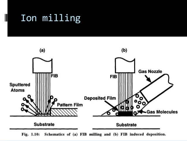
Ion beam etching or milling is achieved by directing a beam of charged particles ions at a substrate with a suitably patterned mask in a high vacuum chamber.
1 512 261 1462 deanturnbaugh ionbeamservices co uk.
Frequently additional information can be obtained on the structure of materials.
Among the dry etching techniques plasma and reactive ion etching are the most popular in semiconductor processing.
Helium ion etching on hsq patterns.
Typical material processes include the precision deposition of thin films remote plasma read more.
In this review the main applications and advantages of using ion beam technology for.
Sometimes the application of this modern etching technique is the sole possibility of making statements.
Find read.
Ion beam application etching or sputtering is a technique conceptually similar to sandblasting but using individual atoms in an ion beam to ablate a target.
Our products are vacuum based process tools which interact with materials at the atomic level.
It enables highly directional beams of neutral ions to control over the sidewall profile as well as radial uniformity optimisation and feature shaping during nanopatterning.
The basic dual ion beam sputtering dibs chamber set up as comprises an etching source that precisely directs a neutralised ion beam onto a wafer located in the substrate holder.
The accuracy of the etching process is considerably high mainly due to the small amount of material removal.
Ion beam services asia pte ltd 1 yishun industrial street 1 a posh bizhub 07 09 singapore 768160 phone.
Tolerances in the vicinity of 50 å 5 x 10 mm are possible.
Product lines kaufman robinson engineers and manufactures broad beam ion and plasma products.
B comparison of helium.
Ion beam services usa inc 22 hedgebrook way austin tx 78738 usa phone.
Ion beam machining accuracy.
.jpg)